A phone’s processor is its heart and its brain. A processor consists of numerous transistors that are built with semiconductor materials like silicon. Transistors are a fundamental element for building modern electronic devices like smartphones.
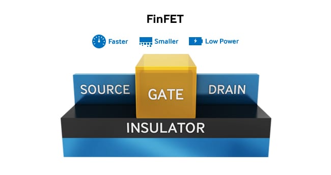
FinFET Process
Out the numerous components in a processor, Fin Field Effect Transistor also known as FinFET transistors are very important. These components help to make even smaller microprocessors, colloquially referred to as extending Moore’s law.
Samsung is one of the top dogs in the semiconductor industry. The company has been the world’s largest memory chip maker since 1993. Samsung Foundry Bussiness has announced that it has now begun mass production of SoCs (System-on-Chip) that are built on its Second Generation 10 Nanometer FinFET process technology, these processors are Low Power Plus too.
Newer SoC’s Performance ramped up!
They say that this revision of the 10nm FinFET process will get the processors 10% higher performance and 15% lower power consumption when compared to its first generation 10nm process technology which was 10LPE (Low Power Early). This was used in numerous flagship processors.
The new process is derived from already successful 10LPE technology. The chip offers competitive advantages by greatly reducing turn-around time from development to mass production and by providing significantly higher initial manufacturing yield.
These SoCs with the 10LPP are set to be released early next year and will be featured on phones that will come out later that year.
“We will be able to better serve our customers through the migration from 10LPE to 10LPP with improved performance and higher initial yield,” said Ryan Lee, vice president of Foundry Marketing at Samsung Electronics. “Samsung with its long-living 10nm process strategy will continue to work on the evolution of 10nm technology down to 8LPP to offer customers distinct competitive advantages for a wide range of applications.”
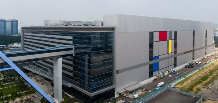
The ‘S3’ Fab Plant
Samsung also said that their newest manufacturing line S3 that is located in Hwaseong, South Korea, is all set to ramp up production of the new 10nm LPP chips. S3 is the third SemiConductor Fabrication Plants from Samsung’s Foundry Business. This is after S1 in Giheung, South Korea, and S2 in Austin, USA. It is also said that Samsung’s 7nm FinFET process technology with Extreme Ultra Violet will also be mass produced here at S3.