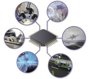
In today’s digital world, our life is surrounded by Embedded Systems. From brewing your morning coffee to microwaving your breakfast to driving your car (with its smart digital features), getting to the office where you take an elevator to get to your smart (auto adjustable) desk.
Systems, Embedded in Our Life
From the auto adjustable desk, you use your laptop for work until you tell Alexa to turn off your smart lamps and head to bed — all the while using your smartphones.
Welcome to the world of Embedded Systems.

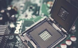
The devices you use are getting smaller, faster, and smarter every day. It’s all happening due to their tiniest component, a semiconductor “Chip,” embedded inside the device. These microchips are smaller than our fingernails. Moreover, almost all the modern-day embedded devices use these Microchips. It’s hard even to imagine a world without them.
The “Brain” in the System
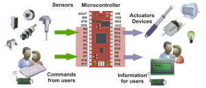
The components of embedded systems consist of Sensors to capture the input signals, a Processor (Microcontroller or “Logic”) to manage the sensors, a memory to store the data, and an actuator or the output device to trigger or capture the results seamlessly. It’s quite the same as our human body. We have sensors (like ears, nose, eyes, etc.), a “Brain” to Process and Memorize, and the rest of our bodies that react.
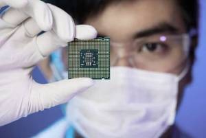
The semiconductor “Chip” (Microcontroller, Processor & Memory) is the “Brain” of the embedded systems. These semiconductor chips are classified as the “Logic” (also known as Processors) and the “Memory.”
The “Need for Speed”
The newer technologies (such as IoT, Machine Learning, Artificial Intelligence, Big Data, and cloud computing) use complex algorithms and need a high-speed processor and faster memory.
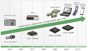
The computation speed and memory requirements are increasing rapidly from supercomputers to smartphones. The first supercomputer, CDC (Control Data Corporation-6600), had a top speed of 40 MHz, which is painfully slow in today’s world.
The first version of a Raspberry Pi (the most straightforward microcontroller, costing less than $50) has a 700-MHz processor. MHz is the ‘clock’ speed of a processor. One million decisions made in a second is one MH. The latest supercomputer can compute 200,000 trillion calculations per second. The iPhone-13 uses an A15 Bionic processor chip having 15 billion transistors.

This also applies to personal computers and laptops. On October 27, 2021, Intel announced its 12th generation processor family, “Core i9-12900K,” the best gaming processor (5.2 GHz), having as many as 16 cores and 24 threads. The new desktop processors reach new heights of multi-threaded performance for enthusiast gamers and professional creators.
Evolution of the next-generation computing
The evolution of advanced semiconductor chips helps devices achieve high-end algorithms. These complex algorithms have been in existence for decades. However, they could not be implemented to their fullest extent in the real world due to the lack of specialized computational tools.
One of the most revolutionary signal processing concepts, the “Fourier Transform” (included in the Top 10 Algorithms of 20th Century by the IEEE) and one of the most critical algorithms used in image processing and telecommunication, has existed for a long time.
Fourier Transform was first discussed in 1805. It’s a mathematical function that transforms a signal from the time domain to the frequency domain. It is a very powerful transformation that gives you the ability to understand the frequencies inside a signal.
However, due to the lack of in-depth computational tools, scientists could not explore it further (until ~1970) or use it in any commercial systems. But now, it’s widely used in image processing and signal processing in many commercial and critical systems (including RADAR & SONAR).
It’s all Happening here, Moore’s law
Gordon Earle Moore is an American engineer and the co-founder and chairman emeritus of Intel Corporation. In 1965, he authored Moore’s law and, using existing data, extrapolated that the number of transistors in integrated circuits (IC) would double about every two years with the reducing costs.
Advancements in the semiconductor manufacturing process (especially the lithography machines) keep Moore’s law alive. In the last few decades, these chips are getting more condensed, efficient, and economical with an increasing number of transistors fabricated in a single monolithic Chip, and the trend continues.
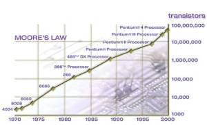
source: https://www.singularitysymposium.com/moores-law.html
The latest technologies evolve in parallel with the semiconductor “Chip” evolutions. As a result, the embedded systems world is getting advanced, smart, and more affordable.
The semiconductor technology revolution produces high-computational, high-speed processors and faster-access memory semiconductor chips. These revolutions are the reason behind the success of the latest technologies, including smartphones.
The success is because the need for critical and optimized signal processing algorithms evolved the concept of “System on Chip” (SoC), where the entire digital and analog signal processing algorithms are done inside the hardware (semiconductor chip) itself.
SoC has managed to make embedded systems more efficient. In addition, these SoC have helped tremendously in overcoming network incompatibility, integration, and reliability issues in IoT, especially in wireless connectivity and 5G capabilities.
These advancements in semiconductor chips have significantly impacted our human life. Their contribution to medical science, from the most straightforward contactless thermometer to the sophisticated life-saving devices, is vast. These advancements have made a tremendous impact in the medical world.
The Chip Shortage, A Current Problem
In recent years, the world has witnessed high-speed digitization and, further boosted by the pandemic, a massive surge in demand for laptops, smartphones, automobiles, and servers. Unfortunately, this has led to a significant problem: a shortage in the chips that control everything.
In addition, the evolving technologies are more demanding, creating the need for smaller, faster processors and more available memory. It’s almost a chicken and egg problem that works to meet production needs.
The current pandemic impacted semiconductor manufacturing in an unprecedented way. However, smart embedded devices have helped keep life going. Our kids continued their education remotely using chrome books, cameras, and headphones, and many workers continued to work remotely without hiccups.
The role of contactless temperature scanners, smart contact tracing using mobile data, and other technologies played an instrumental role in confining the spread of COVID-19. Without these smart embedded systems devices, our life could have been much worse in the past few years.
The Journey and Evolution of the Semiconductor Chip
The semiconductor chip journey started with the “vacuum tubes.” Ancient computers used vacuum tubes. A vacuum tube is a glass tube with electrodes for controlling electron flow, acting as a switch or an amplifier.
In 1947, the University of Pennsylvania made a computer using vacuum tubes almost the size of a building. In the following years, scientists William Shockley, John Bardeen, and Walter Brattain collaborated to invent transistors, to replace the vacuum tube, offering a more effective way for the computer to process information.
Source: https://www.hitachi-hightech.com/global/products/device/semiconductor/history.html
The invention of “Transistors” was a huge milestone and revolutionized semiconductor technology. In addition, it helped in making the integrated circuits smaller, faster, and more affordable. The great researchers “Shockley,” “Bardeen,” and “Brattain” made a considerable contribution to semiconductor research and the development of the transistor and were awarded Nobel Prize in Physics in 1956.
These transistors started getting used in the Integrated Circuits, which are also called “microelectronic circuits,” “microchips,” or “chips.”
The chips are an assembly of electronic components, fabricated as a single unit, in which miniaturized active devices (e.g., transistors and diodes) and passive devices (e.g., capacitors and resistors) along with their interconnections are built upon a thin substrate of semiconductor material (typically silicon).
The resulting circuit is thus a small monolithic “Chip” that we know today.
Chip Manufacturing, Impossible is Past
A chip is a set of electronic circuits where the transistors turn a current on or off. Microchips are made by building up layers of these interconnected patterns of transistors on a silicon wafer. The latest monolithic chips can support more than 100 layers containing a billion transistors each, each aligning at atomic (nanometer), which needs to align with nanometer precision (called ‘overlay’).
The manufacturing process of these semiconductor chips has several steps. Using various automation processes, it can take months from design to mass production in the cleanrooms of the chipmakers’ fabs (fabrication facilities). There are four unique phases in production.
Design Phase: Circuit Design
Development Phase: Printing circuit to a Silicon wafer
Pilot Phase: Critical Production criteria (based on the overlay, critical dimensions, etc.) matching
Mass production Phase: The primary focus is to maximize the yield and minimize the loss (failures) for commercial viability
The Game Changer, EUV Lithography
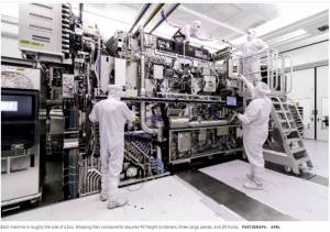
Lithography is when a light source is used to print tiny patterns of devices, including transistors on silicon. It is a fundamental step in a mass-producing microchip. Lithography machines where the hardware meets software provide a holistic approach to mass-producing patterns on silicon. This machine is one of the most complex machines globally, which has evolved tremendously in the past few decades.
ASML (ASML Holding NV) is the market leader in the DUV (Deep Ultraviolet) lithography machines and the only maker of the next generation EUV (Extreme Ultraviolet) lithography machines in the world.
These machines are so complex (almost the size of a bus), with over 100,000 components and around a mile’s length of cable, all assembled to make a giant lithography machine costing more than $150 million per machine.
The precision of these machines is in the nanometer range. For example, ASML uses DUV machines with a precision of around 200 nanometers wavelength. There are only a few DUV manufacturers (Nikon & Canon) other than ASML.
In addition, ASML has been playing an instrumental role in meeting the challenging demand for the latest technologies and keeping Moore’s law alive. For example, ASML’s EUV lithography machine is the next-generation high-resolution lithography machine that made a revolutionary change in achieving a 10-nanometer (almost X-ray range) precision wavelength, something unprecedented in most cases.
ASML invested more than 17 years and approximately 6 billion euros in research and development in making the EUV lithography machines. These EUV machines manufacture sophisticated microchips. The EUV machine is directly benefitting all human beings.
These microchips are used in all the latest smartphones, gaming consoles, smartwatches, and other high-end embedded devices.
The Future is here, EXE Lithography Machines
ASML is working on its next generation of EUV lithography (EXE) machine, which will open the door for a smarter digital world in future decades. Intel and ASML are working together to make it a reality as soon as 2025, and they’ve managed to offer EUV production with numbers that were not possible before.
Above all, the EXE EUV machine would reduce the costs and energy needed to manufacture this chip. This machine also offers to scale at an affordable pace, well into the oncoming decade. This machine has a higher resolution that will enable 1.7x smaller chip features and 2.9x increased chip density.
The number of process steps will reduce significantly with this platform, which is a solid motivation to adopt the technology. In addition, it will significantly reduce defects, costs, and cycle time.

Source: innovationorigins.com/app/uploads/2018/01/ASML-transistor-per-mm2-Wet-van-Moore.png
Epilogue, Techno-Logical
The entire world of technology is evolving in a feedback loop. For example, the need for faster and more efficient hardware (logic & memory chips) used in the latest technology drives the “Chip” fabrication industry.
And the advancement in semiconductor chip manufacturing further pushes the latest technologies forward. For example, the latest (EXE) lithography machines use the most sophisticated semiconductor “chips,” fabricated using the earlier generation Lithography (DUV/EUV) Machines.
The semiconductor “Chip” (logic & memory) advancements are shaping future technologies. While most of this will depend on how efferently we continue to advance the chip manufacturing industry. These challenges could bring about future technology up to this point unprecedented.
We see a significant evolution happening faster than ever before, creating an “industrial revolution” in Embedded Systems.
Disclaimer: Opinions expressed are the author’s own and not the views of his employer.
Inner Article Image Credit: Provided by the Author; Thank you!
Top Image Credit: Jeremy Waterhouse; Pexels; Thank you!